


Molded Interconnect Devices (MID)

Reduce Product Complexity - Shorten Prototype Development Time

Molded Interconnect Devices are electronic components and circuitry integrated onto a plastic housing or base substrate which is both the circuit board and the package of the final product. This process eliminates the need to produce and mount a separte PCB onto the product package and can be used to further minaturise a product into a useful and compact form factor.

In the LDS process, the conductor-path layout is written by laser onto the molded 3D plastic part. The conductor paths are constructed with an electroless metallization process.
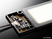
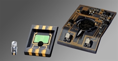
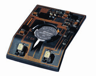
Above are some examples of products which have been made using the LDS process to create circuit paths and mount components onto the base package. Using this process can provide a degree of design freedom not available in the standard PCB on FR4 process.
This may be the solution to reduce your design constraints. Give us a call to see what we can do to help you speed your product to market. LDS can be used for reducing your product development time and for intricate hard to duplicate products.

115 Pleasant Street, Millis MA 02054
Tel 508 794 1283 Fax. 508 376 2505
e mail 2e@2esyscom.com
Tel 508 794 1283 Fax. 508 376 2505
e mail 2e@2esyscom.com